


学術研究員
清水 康雄 / SHIMIZU, Yasuo
東北大学 金属材料研究所 材料照射工学研究部門
〒311-1313 茨城県東茨城郡大洗町成田町2145-2
Phone: 029-267-3181, Fax: 029-267-4947
>> English page
● 研 究 紹 介 ●
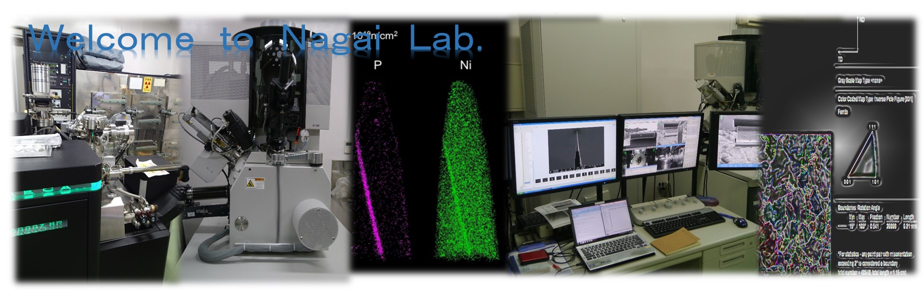
3次元アトムプローブ法を用いて、シリコンやゲルマニウムなどの半導体を基盤とするトランジスタ構造の評価を行っています。 3次元アトムプローブ法は固体材料中の原子1個1個を実空間且つ原子レベルで観測できる手法 であり、今後は多種多様な材料の評価が期待されています。この一連の研究を通じて、固体中の原子間の相互作用や不純物原子クラスター形成メカニズムなどの基礎的な物理現象の解明を目指しています。 最近では、半導体材料のみならず、これまで測定が難しいとされてきた絶縁体・セラミック材料の評価にも取り組んでいます。
半導体関連の3次元アトムプローブ評価の詳細は、解説論文:
をご覧下さい。
● ニ ュ ー ス ●(2020.3.2更新)
【会議・研究会・セミナー】
【論文】
☆ 書籍の紹介 ☆
3次元アトムプローブ法を用いて、シリコンやゲルマニウムなどの半導体を基盤とするトランジスタ構造の評価を行っています。 3次元アトムプローブ法は固体材料中の原子1個1個を実空間且つ原子レベルで観測できる手法 であり、今後は多種多様な材料の評価が期待されています。この一連の研究を通じて、固体中の原子間の相互作用や不純物原子クラスター形成メカニズムなどの基礎的な物理現象の解明を目指しています。 最近では、半導体材料のみならず、これまで測定が難しいとされてきた絶縁体・セラミック材料の評価にも取り組んでいます。
半導体関連の3次元アトムプローブ評価の詳細は、解説論文:
- 3次元アトムプローブによる半導体ナノ構造の元素分布解析
日本真空学会誌 解説 第56巻, 第9号, pp. 340-347 (2013).
- Industrial application of atom probe tomography to semiconductor devices
Scripta Materialia, Vol. 148, pp. 82-90 (2018).
をご覧下さい。
● ニ ュ ー ス ●(2020.3.2更新)
【会議・研究会・セミナー】
- 第67回応用物理学会春季学術講演会(上智大学四谷キャンパス、2020.3.12-15開催)に参加予定でした。
- MRS Fall Meeting & Exhibit 2019(ボストン、米国、2019.12.1-6開催)にて発表しました。
- 第22回二次イオン質量分析国際会議(SIMS22)(みやこめっせ、京都、2019.10.20-25開催)にて発表しました。
【論文】
- 大阪市立大学との共同研究で、常温で直接接合した銅-ダイヤモンド界面のナノ構造評価(熱処理の効果)について、ACS Applied Nano Materials誌に掲載されました。
- 慶應義塾大学と東北大学国際集積エレクトロニクス研究開発センターとの共同研究で、酸化シリコンナノピラー中のシリコン自己拡散評価について、Journal of Applied Physics誌に掲載されました。
- 香港城市大学との共同研究で、FeCoNiCrTi0.2の機械的特性およびアトムプローブ評価について、Acta Materialia誌に掲載されました。
☆ 書籍の紹介 ☆
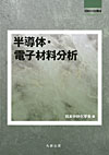
試料分析講座 半導体・電子材料分析
ISBN978-4-621-08700-8, 日本分析化学会編, 丸善出版 (2013年7月発売)
ISBN978-4-621-08700-8, 日本分析化学会編, 丸善出版 (2013年7月発売)
第6章 三次元アトムプローブ(APT)を執筆しました。APT法の測定原理や試料準備方法をはじめ、半導体・電子材料の量子デバイス構造における最近の測定例について解説した数少ない和書です。
本書では、デバイスの開発、製造ラインの立ち上げ、歩留まり向上、不良解析のための形態観察、汚染元素検出、欠陥解析などに用いられる分析法について、その原理・特長および応用例を紹介しています。
ぜひこちらをご覧下さい。
● 職 歴 ●
● 外 部 委 員 ●
● 学 歴 ●
- 2020.4- 2020.4東北大学 金属材料研究所 学術研究員
- 2010.4- 2020.3東北大学 金属材料研究所 材料照射工学研究部門 助教
- 2009.4- 2010.1Post-Doctoral Researcher
Department of Metallurgy and Materials Engineering
Katholieke Universiteit Leuven (Belgium) and IMEC vzw - 2008.4- 2010.3独立行政法人日本学術振興会 特別研究員
- 2007.10- 2009.3慶應義塾大学大学院 グローバルCOE RA研究員
● 外 部 委 員 ●
- 2018.10- 現在Program Committee
22nd International Conference on SIMS - 2017.4- 現在システムデバイスロードマップ(SDRJ)委員会委員
ワーキンググループ:Metrology - 2016.6- 2017.8Local Program Sub-Committee (Materials Characterization)
International Conference on Defects in Semiconductors - 2014.4- 現在SIMS国際シンポジウム(SISS)幹事会委員
- 2014.6- 2016.3電子情報技術産業協会半導体技術ロードマップ専門委員会
専門部会WG14(計測)特別委員
● 学 歴 ●
- 2006.4- 2009.3慶應義塾大学大学院 理工学研究科
基礎理工学専攻 博士課程 [博士(工学)] - 2004.4- 2006.3慶應義塾大学大学院 理工学研究科 基礎理工学専攻 修士課程
- 2000.4- 2004.3慶應義塾大学 理工学部 学門1(物理情報工学科)
● 受 賞 ●
● 競争的資金・助成金 ●

日本の研究.com
【代表者】
- 2017.4Poster Award/64th JSAP Spring Meeting 2017(筆頭:Yuan TU)
- 2016.6Best Poster Award/Atom Probe Tomography & Microscopy 2016
- 2013.5優秀ポスター賞/第125回2013年春季東北大学金属材料研究所講演会
- 2012.11MRS Outstanding Poster Award
Materials Research Society (MRS) Fall Meeting 2012 - 2011.3MIRAI賞最優秀賞/次世代半導体材料・プロセス基盤プロジェクト
- 2009.3Distinguished Research Associate 2008/Keio G-COE Program
- 2008.3First Prize/Keio-Gent G-COE Joint Workshop for Future Network
- 2008.3First Prize/Final Report 2007 in Keio G-COE Program
- 2007.11Student Award/第16回二次イオン質量分析に関する国際会議
- 2006.8第20回応用物理学会講演奨励賞/第53回春季応用物理学関係連合講演会
- 2006.3専修主任賞/慶應義塾大学大学院理工学研究科 基礎理工学専攻 応用物理専修
● 競争的資金・助成金 ●
日本の研究.com
【代表者】
学術研究助成基金助成金・基盤研究(C) [2020-2022年度]
科学研究費補助金・若手研究(A) [2015-2017年度]
学術研究助成基金助成金・挑戦的萌芽研究 [2014-2015年度]
学術研究助成基金助成金・若手研究(B) [2012-2013年度]
公益財団法人カシオ科学振興財団第29回研究助成 [2011年度]
STARC研究テーマアイデア・スカウト(IS)プログラム [2011年度]
第1回優秀若手研究者海外派遣事業 [2009年度]
科学研究費補助金・特別研究員奨励費 [2008-2009年度]
【分担者として参画】科学研究費補助金・若手研究(A) [2015-2017年度]
学術研究助成基金助成金・挑戦的萌芽研究 [2014-2015年度]
学術研究助成基金助成金・若手研究(B) [2012-2013年度]
公益財団法人カシオ科学振興財団第29回研究助成 [2011年度]
STARC研究テーマアイデア・スカウト(IS)プログラム [2011年度]
第1回優秀若手研究者海外派遣事業 [2009年度]
科学研究費補助金・特別研究員奨励費 [2008-2009年度]
科学研究費補助金・基盤研究(A)(代表者:永井康介) [2020-2023年度(予定)]
国家課題対応型研究開発推進事業原子力システム研究開発事業(安全基盤技術研究開発)
(代表者:永井康介) [2018-2021年度(予定)]
科学研究費補助金・基盤研究(A)(代表者:品田賢宏) [2018-2022年度(予定)]
科学研究費補助金・基盤研究(A)(代表者:永井康介) [2016-2018年度]
科学研究費補助金及び学術研究助成基金助成金・基盤研究(B)
(代表者:井上耕治) [2014-2016年度]
国家課題対応型研究開発推進事業原子力システム研究開発事業(安全基盤技術研究開発)
(代表者:永井康介) [2012-2015年度]
科学研究費補助金・基盤研究(A)(代表者:永井康介) [2012-2014年度]
科学研究費補助金・基盤研究(A)(代表者:永井康介) [2010-2011年度]
国家課題対応型研究開発推進事業原子力システム研究開発事業(安全基盤技術研究開発)
(代表者:永井康介) [2018-2021年度(予定)]
科学研究費補助金・基盤研究(A)(代表者:品田賢宏) [2018-2022年度(予定)]
科学研究費補助金・基盤研究(A)(代表者:永井康介) [2016-2018年度]
科学研究費補助金及び学術研究助成基金助成金・基盤研究(B)
(代表者:井上耕治) [2014-2016年度]
国家課題対応型研究開発推進事業原子力システム研究開発事業(安全基盤技術研究開発)
(代表者:永井康介) [2012-2015年度]
科学研究費補助金・基盤研究(A)(代表者:永井康介) [2012-2014年度]
科学研究費補助金・基盤研究(A)(代表者:永井康介) [2010-2011年度]
● 招 待 講 演 ●
- Dopant behavior in semiconductor materials and nanostructures analyzed by atom probe tomography
第19回「イオンビームによる表面・界面解析」特別研究会
京都大学宇治キャンパス, 2018年12月.
- Atom probe study of silicon-based device structures
Atom Probe Tomography and Microscopy (APT&M) 2018, NIST, Gaithersburg, Maryland, USA, June 2018.
- 3次元アトムプローブ法を用いた材料解析:原理と応用
日本学術振興会 結晶加工と評価技術 第145委員会 第156回研究会
明治大学駿河台キャンパス グローバルフロント, 2017年12月.
- Atom probe study of semiconductor-based nanostructure
IUMRS-ICAM 2017, Kyoto University, August 2017.
- Dopant detection in silicon nanostructures by atom probe tomography
4th Bilateral Italy-Japan Seminar: Innovative Solutions for Single Atom Applications in Photonics and Nanoelectronics, Colico, Lago di Como, Italy, May 2017.
- Atom probe tomography of semiconductor and oxide materials
第26回日本MRS年次大会, 横浜, 2016年12月.
- 先端デバイス開発のための3次元アトムプローブ分析技術の応用例
カメカテクニカルセミナー2016 [プログラムPDF版]
くるまプラザ(港区芝大門), 2016年11月.
- 先端ナノエレクトロニクス材料の元素分布分析
第106回総研セミナー, 東京都市大学 総合研究所, 2016年4月.
- 3D-APの半導体応用の現状と最近の話題
日本学術振興会 ナノプローブテクノロジー 第167委員会 第81回研究会
東京大学駒場キャンパス コンベンションホール, 2016年1月.
- 半導体デバイス中のドーパント分布解析に向けた3次元アトムプローブの利用
電子情報技術産業協会(JEITA)半導体技術ロードマップ専門委員会(STRJ)
故障解析SWG 第62回会合, メルパルク京都, 2015年12月.
- Panel Session: Dopant Visualization
第35回ナノテスティングシンポジウム (NanoTS 2015)
千里ライフサイエンスセンター, 2015年11月.
- Elemental distributions in semiconductor-based device structures analyzed by atom probe tomography
2015 International Symposium for Advanced Materials Research (ISAMR), Sun Moon Lake, Taiwan, August 2015.
- 3D atomic-scale-analysis of elemental distribution in silicon nanoelectronics
3rd Bilateral Italy-Japan Seminar: Silicon Nanoelectronics for Advanced Applications, Campus Plaza Kyoto, Japan, June 2015.
- 3次元アトムプローブを用いた材料中の元素分布評価 ~半導体を例に~
一般財団法人 材料科学技術振興財団, 2015年2月.
- 3次元アトムプローブを用いた材料解析例
電子顕微鏡解析技術分科会フォーラム [プログラムPDF版], 時之栖, 2014年8月.
- Assessment of tooth composition by atom probe tomography
Student Chapter Research Meeting
Tokyo Medical and Dental University, June 2014.
- 3次元アトムプローブによる半導体材料・デバイス中の元素分布評価~アトムプローブの標準化活動を念頭に~
表面化学分析技術国際標準化委員会(JSCA)WG
東京八重洲ホール, 2013年12月.
- 3次元アトムプローブによる半導体ナノ構造中の元素分布評価例
カメカテクニカルセミナー2013 [プログラムPDF版]
くるまプラザ(港区芝大門), 2013年11月.
- 3次元アトムプローブによる半導体デバイス中のドーパント分布解析
日本学術振興会 材料の微細組織と機能性 第133委員会 第218回研究会
東京工業大学キャンパス イノベーションセンター, 2013年10月.
- Elemental distribution analysis in semiconductor-based MOS devices with atom probe tomography
2013 JSAP-MRS Symposia
Doshisha University, Kyoto, Japan, September 2013.
- 半導体デバイスの3次元アトムプローブ解析
第29回分析電子顕微鏡討論会, 幕張メッセ国際会議場, 2013年9月.
- Dopant analysis of semiconductor devices with atom probe tomography
15th International Symposium on SIMS and Related Techniques Based on Ion-Solid Interactions at Seikei University (SISS-15)
Tokyo, Japan, April 2013.
- 3次元アトムプローブによる半導体デバイス中の元素分布解析
電子情報技術産業協会(JEITA)半導体技術ロードマップ専門委員会(STRJ)
WG14専門部会(メトロロジ:計測WG), JEITA会議室, 2013年1月.
- 三次元アトムプローブによるシリコンMOSデバイス材料の評価
カメカテクニカルセミナー2011, くるまプラザ(港区芝大門), 2011年11月.
- Characterization of three-dimensional dopant distribution in MOSFETs by atom probe
1st Annual World Congress of Nano-S&T
The Dalian World Expo Center, Dalian, China, October 2011.
- 3D-AP法によるSi-MOSFET中不純物分布解析
日本学術振興会 ナノプローブテクノロジー 第167委員会 第63回研究会
慶應義塾大学日吉キャンパス, 2011年7月.
- CMOS process monitoring using silicon isotopes
Companion Workshop "Impact of METROLOGY on TCAD" in 2008 International Conference on Simulation of Semiconductor Processes and Devices, Hakone, Japan, September 2008.
● 論 文 ●
更新日: 2020年4月2日
| Publons | ORCID | ResearchGate | Scopus | Google Scholar | researchmap | Dimensions |
● 知 的 財 産 権 ●
更新日: 2020年4月2日
| Publons | ORCID | ResearchGate | Scopus | Google Scholar | researchmap | Dimensions |
- Characterization of nanoscopic Cu/diamond interfaces prepared by surface activated bonding: Implications for thermal management
J. Liang, Y. Ohno, Y. Yamashita, Y. Shimizu, S. Kanda, N. Kamiuchi, S.-W. Kim , K. Koyama, Y. Nagai, M. Kasu, and N. Shigekawa
ACS Applied Nano Materials, Vol. 3, Issue 3, pp. 2455-2462 (2020).
- Oxidation-enhanced Si self-diffusion in isotopically modulated silicon nanopillars
R. Kiga, S. Hayashi, S. Miyamoto, Y. Shimizu, Y. Nagai, T. Endoh, and K. M. Itoh
Journal of Applied Physics, Vol. 127, Issue 4, 045704 (2020) (6 pages).
- Impact of focused ion beam on structural and compositional analysis of interfaces fabricated by surface activated bonding
Y. Ohno, H. Yoshida, N. Kamiuchi, R. Aso, S. Takeda, Y. Shimizu, Y. Nagai, J. Liang, and N. Shigekawa
Japanese Journal of Applied Physics, Vol. 59, No. SB, SBBB05 (2020) (5 pages).
- Fabrication of diamond/Cu direct bonding for power device applications
S. Kanda, Y. Shimizu, Y. Ohno, K. Shirasaki, Y. Nagai, M. Kasu, N. Shigekawa, and J. Liang
Japanese Journal of Applied Physics, Vol. 59, No. SB, SBBB03 (2020) (5 pages).
- 2019 -
- Atom probe tomography of GaAs homointerfaces fabricated by surface-activated bonding
Y. Shimizu, N. Ebisawa, Y. Ohno, J. Liang, N. Shigekawa, K. Inoue, and Y. Nagai
Proceedings of 2019 6th International Workshop on Low Temperature Bonding for 3D Integration (LTB-3D), p. 56, ISBN: 978-4-9047-4307-2
- Artifacts in the structural analysis of SAB-fabricated interfaces by using focused ion beam
Y. Ohno, H. Yoshida, N. Kamiuchi, R. Aso, S. Takeda, Y. Shimizu, N. Ebisawa, Y. Nagai, J. Liang, and N. Shigekawa
Proceedings of 2019 6th International Workshop on Low Temperature Bonding for 3D Integration (LTB-3D), p. 55, ISBN: 978-4-9047-4307-2
- Outstanding tensile properties of a precipitation-strengthened FeCoNiCrTi0.2 high-entropy alloy at room and cryogenic temperatures
Y. Tong, D. Chen, B. Han, J. Wang, R. Feng, T. Yang, C. Zhao, Y. L. Zhao, W. Guo, Y. Shimizu, C. T. Liu, P. K. Liaw, K. Inoue, Y. Nagai, A. Hu, and J. J. Kai
Acta Materialia, Vol. 165, pp. 228-240 (2019).
- 2018 -
- Effect of carbon on boron diffusion and clustering in silicon: Temperature dependence study
Y. Tu, Y. Shimizu, Y. Kunimune, Y. Shimada, T. Katayama, T. Ide, M. Inoue, F. Yano, K. Inoue, and Y. Nagai
Journal of Applied Physics, Vol. 124, Issue 15, 155702 (2018) (8 pages).
- Industrial application of atom probe tomography to semiconductor devices
A. D. Giddings, S. Koelling, Y. Shimizu, R. Estivill, K. Inoue, W. Vandervorst, and W. K. Yeoh
Scripta Materialia, Vol. 148, pp. 82-90 (2018).
Viewpoint set
- Composition evolution of gamma prime nanoparticles in the Ti-doped CoFeCrNi high entropy alloy
B. Han, J. Wei, Y. Tong, D. Chen, Y. Zhao, J. Wang, F. He, T. Yang, C. Zhao, Y. Shimizu, K. Inoue, Y. Nagai, A. Hu, C.-T. Liu, and J.-J. Kai
Scripta Materialia, Vol. 148, pp. 42-46 (2018).
- Blocking of deuterium diffusion in poly-Si/Al2O3/HfxSi1-xO2/SiO2 high-k stacks as evidenced by atom probe tomography
Y. Tu, B. Han, Y. Shimizu, Y. Kunimune, Y. Shimada, T. Katayama, T. Ide, M. Inoue, F. Yano, K. Inoue, and Y. Nagai
Applied Physics Letters, Vol. 112, Issue 3, 032902 (2018) (5 pages).
- 2017 -
- Nanoscopic analysis of oxygen segregation at tilt boundaries in silicon ingots using atom probe tomography combined with TEM and ab initio calculations
Y. Ohno, K. Inoue, K. Fujiwara, K. Kutsukake, M. Deura, I. Yonenaga, N. Ebisawa, Y. Shimizu, K. Inoue, Y. Nagai, H. Yoshida, S. Takeda, S. Tanaka, and M. Kohyama
Journal of Microscopy, Vol. 268, Issue 3, pp. 230-238 (2017).
- 1.54 μm photoluminescence from Er:Ox centers at extremely low concentration in silicon at 300 K
M. Celebrano, L. Ghirardini, M. Finazzi, Y. Shimizu, Y. Tu, K. Inoue, Y. Nagai, T. Shinada, Y. Chiba, A. Abdelghafar, M. Yano, T. Tanii, and E. Prati
Optics Letters, Vol. 42, Issue 17, pp. 3311-3314 (2017).
arXiv: 1702.00331
- Atom probe tomographic assessment of the distribution of germanium atoms implanted in a silicon matrix through nano-apertures
Y. Tu, B. Han, Y. Shimizu, K. Inoue, Y. Fukui, M. Yano, T. Tanii, T. Shinada, and Y. Nagai
Nanotechnology, Vol. 28, No. 38, 385301 (2017) (7 pages).
- Revisiting room-temperature 1.54 μm photoluminescence of ErOx centers in silicon at extremely low concentration
E. Prati, M. Celebrano, L. Ghirardini, P. Biagioni, M. Finazzi, Y. Shimizu, Y. Tu, K. Inoue, Y. Nagai, T. Shinada, Y. Chiba, A. Abdelghafar, M. Yano, and T. Tanii
Proceedings of 2017 Silicon Nanoelectronics Workshop (SNW), pp. 105-106, ISSN 2161-4644
- Atom probe study of erbium and oxygen co-implanted silicon
Y. Shimizu, Y. Tu, A. Abdelghafar, M. Yano, Y. Suzuki, T. Tanii, T. Shinada, E. Prati, M. Celebrano, M. Finazzi, L. Ghirardini, K. Inoue, and Y. Nagai
Proceedings of 2017 Silicon Nanoelectronics Workshop (SNW), pp. 99-100, ISSN 2161-4644
- Impact of local atomic stress on oxygen segregation at tilt boundaries in silicon
Y. Ohno, K. Inoue, K. Fujiwara, K. Kutsukake, M. Deura, I. Yonenaga, N. Ebisawa, Y. Shimizu, K. Inoue, Y. Nagai, H. Yoshida, S. Takeda, S. Tanaka, and M. Kohyama
Applied Physics Letters, Vol. 110, Issue 6, 062105 (2017) (5 pages).
- Weak-beam scanning transmission electron microscopy for quantitative dislocation density measurement in steels
K. Yoshida, M. Shimodaira, T. Toyama, Y. Shimizu, K. Inoue, T. Yoshiie, K. J. Milan, R. Gerard, and Y. Nagai
Microscopy, Vol. 66, Issue 2, pp. 120-130 (2017).
EDITOR'S CHOICE
- Influence of laser power on atom probe tomographic analysis of boron distribution in silicon
Y. Tu, H. Takamizawa, B. Han, Y. Shimizu, K. Inoue, T. Toyama, F. Yano, A. Nishida, and Y. Nagai
Ultramicroscopy, Vol. 173, pp. 58-63 (2017).
- 2016 -
- Boron distributions in individual core-shell Ge/Si and Si/Ge heterostructured nanowires
B. Han, Y. Shimizu, J. Wipakorn, K. Nishibe, Y. Tu, K. Inoue, N. Fukata, and Y. Nagai
Nanoscale, Vol. 8, Issue 47, pp. 19811-19815 (2016).
- Recombination activity of nickel, copper, and oxygen atoms segregating at grain boundaries in mono-like silicon crystals
Y. Ohno, K. Kutsukake, M. Deura, I. Yonenaga, Y. Shimizu, N. Ebisawa, K. Inoue, Y. Nagai, H. Yoshida, and S. Takeda
Applied Physics Letters, Vol. 109, Issue 14, 142105 (2016) (4 pages).
- Predoping effects of boron and phosphorous on arsenic diffusion along grain boundaries in polycrystalline silicon investigated by atom probe tomography
H. Takamizawa, Y. Shimizu, K. Inoue, Y. Nozawa, T. Toyama, F. Yano, M. Inoue, A. Nishida, and Y. Nagai
Applied Physics Express, Vol. 9, No. 10, 106601 (2016) (4 pages).
- Quantitative analysis of hydrogen in SiO2/SiN/SiO2 stacks using atom probe tomography
Y. Kunimune, Y. Shimada, Y. Sakurai, M. Inoue, A. Nishida, B. Han, Y. Tu, H. Takamizawa, Y. Shimizu, K. Inoue, F. Yano, Y. Nagai, T. Katayama, and T. Ide
AIP Advances, Vol. 6, Issue 4, 045121 (2016) (7 pages).
- Suppression of segregation of the phosphorus δ-doping layer in germanium by incorporation of carbon
M. Yamada, K. Sawano, M. Uematsu, Y. Shimizu, K. Inoue, Y. Nagai, and K. M. Itoh
Japanese Journal of Applied Physics, Vol. 55, No. 3, 031304 (2016) (5 pages).
- Impact of carbon co-implantation on boron distribution and activation in silicon studied by atom probe tomography and spreading resistance measurements
Y. Shimizu, H. Takamizawa, K. Inoue, F. Yano, S. Kudo, A. Nishida, T. Toyama, and Y. Nagai
Japanese Journal of Applied Physics, Vol. 55, No. 2, 026501 (2016) (5 pages).
- Evolution of shape, size, and areal density of a single plane of Si nanocrystals embedded in SiO2 matrix studied by atom probe tomography
B. Han, Y. Shimizu, G. Seguini, E. Arduca, C. Castro, G. Ben Assayag, K. Inoue, Y. Nagai, S. Schamm-Chardon, and M. Perego
RSC Advances, Vol. 6, Issue 5, pp. 3617-3622 (2016).
- 2015 -
- Elemental distributions in multilayer systems by laser-assisted atom probe tomography with various analysis directions
M. Kubota, H. Takamizawa, Y. Shimizu, Y. Nozawa, N. Ebisawa, T. Toyama, Y. Ishida, K. Yanagiuchi, K. Inoue, and Y. Nagai
Microscopy and Microanalysis, Vol. 21, Issue 6, pp. 1373-1378 (2015).
- Characterization and process development of CVD/ALD‐based Cu(Mn)/Co(W) interconnect system
K. Shima, Y. Tu, B. Han, H. Takamizawa, H. Shimizu, Y. Shimizu, T. Momose, K. Inoue, Y. Nagai, and Y. Shimogaki
Proceedings of Advanced Metallization Conference (AMC) 2015 [Open Access], ISBN 978‐3‐944640‐97‐6
- Diffusivity and solubility of Cu in a reactor pressure vessel studied by atom probe tomography
M. Shimodaira, T. Toyama, F. Takahama, N. Ebisawa, Y. Nozawa, Y. Shimizu, K. Inoue, and Y. Nagai
Materials Transactions, Vol. 56, No. 9, pp. 1513-1516 (2015).
- Phosphorus and boron diffusion paths in the polycrystalline silicon gate of a trench-type three-dimensional metal-oxide-semiconductor field-effect transistor investigated by atom probe tomography
B. Han, H. Takamizawa, Y. Shimizu, K. Inoue, Y. Nagai, F. Yano, Y. Kunimune, M. Inoue, and A. Nishida
Applied Physics Letters, Vol. 107, Issue 2, 023506 (2015) (4 pages).
- Three-dimensional evaluation of gettering ability for oxygen atoms at small-angle tilt boundaries in Czochralski-grown silicon crystals
Y. Ohno, K. Inoue, K. Fujiwara, M. Deura, K. Kutsukake, I. Yonenaga, Y. Shimizu, K. Inoue, N. Ebisawa, and Y. Nagai
Applied Physics Letters, Vol. 106, Issue 25, 251603 (2015) (4 pages).
- Nanoscopic mechanism of Cu precipitation at small-angle tilt boundaries in Si
Y. Ohno, K. Inoue, K. Kutsukake, M. Deura, T. Ohsawa, I. Yonenaga, H. Yoshida, S. Takeda, R. Taniguchi, H. Otubo, S. R. Nishitani, N. Ebisawa, Y. Shimizu, H. Takamizawa, K. Inoue, and Y. Nagai
Physical Review B, Vol. 91, Issue 23, 235315 (2015) (5 pages).
- Microstructural evolution of RPV steels under proton and ion irradiation studied by positron beam spectroscopy
J. Jiang, Y. C. Wu, X. B. Liu, R. S. Wang, Y. Nagai, K. Inoue, Y. Shimizu, and T. Toyama
Journal of Nuclear Materials, Vol. 458, pp. 326-334 (2015).
- 2014 -
- Role of W and Mn for reliable 1X nanometer-node ultra-large-scale integration Cu interconnects proved by atom probe tomography
K. Shima, Y. Tu, H. Takamizawa, H. Shimizu, Y. Shimizu, T. Momose, K. Inoue, Y. Nagai, and Y. Shimogaki
Applied Physics Letters, Vol. 105, Issue 13, 133512 (2014) (5 pages).
- The diffusivity and solubility of copper in ferromagnetic-iron at lower temperatures studied by atom probe tomography
T. Toyama, F. Takahama, A. Kuramoto, H. Takamizawa, Y. Nozawa, N. Ebisawa, M. Shimodaira, Y. Shimizu, K. Inoue, and Y. Nagai
Scripta Materialia, Vol. 83, pp. 5-8 (2014).
- Effects of post-irradiation annealing and re-irradiation on microstructure in surveillance test specimens of the Loviisa-1 reactor studied by atom probe tomography and positron annihilation
T. Toyama, A. Kuramoto, Y. Nagai, K. Inoue, Y. Nozawa, Y. Shimizu, Y. Matsukawa, M. Hasegawa, and M. Valo
Journal of Nuclear Materials, Vol. 449, Issues 1-3, pp. 207-212 (2014).
- Depth analysis of Ta/NiFe/Ta/CoFeB/Ta/NiFe multilayer thin films: Comparison of atom probe tomography and Auger electron spectroscopy
M. Kubota, Y. Ishida, K. Yanagiuchi, H. Takamizawa, Y. Nozawa, N. Ebisawa, Y. Shimizu, T. Toyama, K. Inoue, and Y. Nagai
Journal of Surface Analysis, Vol. 20, No. 3, pp. 207-210 (2014).
- Behavior of phosphorous and contaminants from monolayer doping combined with a conventional spike annealing method
Y. Shimizu, H. Takamizawa, K. Inoue, F. Yano, Y. Nagai, L. Lamagna, G. Mazzeo, M. Perego, and E. Prati
Nanoscale, Vol. 6, Issue 2, pp. 706-710 (2014).
- 2013 -
- New applications in atom probe tomography
D. J. Larson, J. W. Valley, T. Ushikubo, M. K. Miller, H. Takamizawa, Y. Shimizu, L. M. Gordon, D. Joester, A. D. Giddings, D. A. Reinhard, T. J. Prosa, D. P. Olson, D. F. Lawrence, P. H. Clifton, R. M. Ulfig, I. Y. Martin, and T. F. Kelly
Microscopy and Microanalysis, Vol. 19 (Supplement 2), pp. 1022-1023 (2013).
- Three-dimensional evaluation of gettering ability of Σ3{111} grain boundaries in silicon by atom probe tomography combined with transmission electron microscopy
Y. Ohno, K. Inoue, Y. Tokumoto, K. Kutsukake, I. Yonenaga, N. Ebisawa, H. Takamizawa, Y. Shimizu, K. Inoue, Y. Nagai, H. Yoshida, and S. Takeda
Applied Physics Letters, Vol. 103, Issue 10, 102102 (2013) (4 pages).
- Three-dimensional characterization of deuterium implanted in silicon using atom probe tomography
H. Takamizawa, K. Hoshi, Y. Shimizu, F. Yano, K. Inoue, S. Nagata, T. Shikama, and Y. Nagai
Applied Physics Express, Vol. 6, No. 6, 066602 (2013) (3 pages).
- Three-dimensional dopant characterization in actual metal-oxide-semiconductor devices of 65 nm node by atom probe tomography
K. Inoue, H. Takamizawa, Y. Shimizu, T. Toyama, F. Yano, A. Nishida, T. Mogami, K. Kitamoto, T. Miyagi, J. Kato, S. Akahori, N. Okada, M. Kato, H. Uchida, and Y. Nagai
Applied Physics Express, Vol. 6, No. 4, 046502 (2013) (4 pages).
- Atomic-scale characteriation of germanium isotopic multilayers by atom probe tomography
Y. Shimizu, H. Takamizawa, Y. Kawamura, M. Uematsu, T. Toyama, K. Inoue, E. E. Haller, K. M. Itoh, and Y. Nagai
Journal of Applied Physics, Vol. 113, Issue 2, 026101 (2013) (3 pages).
- 陽電子消滅および3次元アトムプローブによる原子炉圧力容器鋼の照射脆化機構に関する研究 -フィンランド・ロビーザ炉監視試験片を例として-
外山健, 蔵本明, 野沢康子, Matti Valo, 清水康雄, 井上耕治, 長谷川雅幸, 永井康介
日本陽電子科学会会報 陽電子科学 「最近の研究から」 第1号(通算 第5巻, 第2号), pp. 41-46 (2013).
- 3次元アトムプローブによる半導体ナノ構造の元素分布解析
清水康雄, 井上耕治, 高見澤悠, 矢野史子, 永井康介
日本真空学会(Journal of the Vacuum Society of Japan)誌 解説
第56巻, 第9号, pp. 340-347 (2013).
- 2012 -
- Correlation between threshold voltage and channel boron concentration in silicon-based negative-type metal-oxide-semiconductor field-effect transistors studied by atom probe tomography
H. Takamizawa, Y. Shimizu, K. Inoue, T. Toyama, F. Yano, A. Nishida, T. Mogami, N. Okada, M. Kato, H. Uchida, K. Kitamoto, T. Miyagi, J. Kato, and Y. Nagai
Applied Physics Letters, Vol. 100, Issue 25, 253504 (2012) (3 pages).
- Dopant characterization in self-regulatory plasma doped fin field-effect transistors by atom probe tomography
H. Takamizawa, Y. Shimizu, Y. Nozawa, T. Toyama, H. Morita, Y. Yabuuchi, M. Ogura, and Y. Nagai
Applied Physics Letters, Vol. 100, Issue 9, 093502 (2012) (3 pages).
- Investigation of the factors determining the SIMS depth resolution function in silicon-isotope multiple layers
M. Tomita, K. Koike, H. Akutsu, S. Takeno, Y. Kawamura, Y. Shimizu, M. Uematsu, and K. M. Itoh
Journal of Vacuum Science & Technology B, Vol. 30, Issue 1, 011803 (2012) (12 pages).
- レーザー3次元アトムプローブによる半導体材料中のドーパント分布解析
井上耕治, 清水康雄, 高見澤悠
日本物理学会誌「最近の研究から」 第67巻, 第9号, pp. 645-649 (2012).
- 2011 -
- Three-dimensional elemental analysis of commercial 45 nm node device with high-k / metal gate by atom probe tomography
K. Inoue, H. Takamizawa, K. Kitamoto, J. Kato, T. Miyagi, Y. Nakagawa, N. Kawasaki, N. Sugiyama, H. Hashimoto, Y. Shimizu, T. Toyama, Y. Nagai, and A. Karen
Applied Physics Express, Vol. 4, No. 11, 116601 (2011) (3 pages).
- Origin of characteristic variability in metal-oxide-semiconductor field-effect transistors revealed by three-dimensional atom imaging
H. Takamizawa, Y. Shimizu, K. Inoue, T. Toyama, N. Okada, M. Kato, H. Uchida, F. Yano, A. Nishida, T. Mogami, and Y. Nagai
Applied Physics Letters, Vol. 99, Issue 13, 133502 (2011) (3 pages).
- Impact of carbon coimplantation on boron behavior in silicon: Carbon-boron coclustering and suppression of boron diffusion
Y. Shimizu, H. Takamizawa, K. Inoue, T. Toyama, Y. Nagai, N. Okada, M. Kato, H. Uchida, F. Yano, T. Tsunomura, A. Nishida, and T. Mogami
Applied Physics Letters, Vol. 98, Issue 23, 232101 (2011) (3 pages).
- Channel dopant distribution in metal-oxide-semiconductor field-effect transistors analyzed by laser-assisted atom probe tomography
H. Takamizawa, K. Inoue, Y. Shimizu, T. Toyama, F. Yano, T. Tsunomura, A. Nishida, T. Mogami, and Y. Nagai
Applied Physics Express, Vol. 4, No. 3, 036601 (2011) (3 pages).
- Depth and lateral resolution of laser-assisted atom probe microscopy of silicon revealed by isotopic heterostructures
Y. Shimizu, Y. Kawamura, M. Uematsu, M. Tomita, T. Kinno, N. Okada, M. Kato, H. Uchida, M. Takahashi, H. Ito, H. Ishikawa, Y. Ohji, H. Takamizawa, Y. Nagai, and K. M. Itoh
Journal of Applied Physics, Vol. 109, Issue 3, 036102 (2011) (3 pages).
- 2010 -
- Critical displacement of host-atoms for amorphization in germanium induced by arsenic implantation
Y. Kawamura, Y. Shimizu, H. Oshikawa, M. Uematsu, E. E. Haller, and K. M. Itoh
Applied Physics Express, Vol. 3, No. 7, 071303 (2010) (3 pages).
- 2009 -
- Quantitative evaluation of germanium displacement induced by arsenic implantation using germanium isotope superlattices
Y. Kawamura, Y. Shimizu, H. Oshikawa, M. Uematsu, E. E. Haller, and K. M. Itoh
Physica B: Condensed Matter, Vol. 404, Issues 23-24, pp. 4546-4548 (2009).
- Atom probe microscopy of three-dimensional distribution of silicon isotopes in 28Si/30Si isotope superlattices with sub-nanometer spatial resolution
Y. Shimizu, Y. Kawamura, M. Uematsu, K. M. Itoh, M. Tomita, M. Sasaki, H. Uchida, and M. Takahashi
Journal of Applied Physics, Vol. 106, Issue 7, 076102 (2009) (3 pages).
- Probing the behaviors of point defects in silicon and germanium using isotope superlattices
M. Uematsu, M. Naganawa, Y. Shimizu, K. M. Itoh, K. Sawano, Y. Shiraki, and E. E. Haller
ECS Transactions, Vol. 25, Issue 3, pp. 51-54 (2009).
- Behaviors of neutral and charged silicon self-interstitials during transient enhanced diffusion in silicon investigated by isotope superlattices
Y. Shimizu, M. Uematsu, K. M. Itoh, A. Takano, K. Sawano, and Y. Shiraki
Journal of Applied Physics, Vol. 105, Issue 1, 013504 (2009) (6 pages).
- 2008 -
- Silicon isotope superlattices: Ideal SIMS standards for shallow junction characterization
Y. Shimizu, A. Takano, and K. M. Itoh
Applied Surface Science, Vol. 255, Issue 4, pp. 1345-1347 (2008).
- Film thickness determinating method of the silicon isotope superlattices by SIMS
A. Takano, Y. Shimizu, and K. M. Itoh
Applied Surface Science, Vol. 255, Issue 4, pp. 1430-1432 (2008).
- Charge states of vacancies in germanium investigated by simultaneous observation of germanium self- and arsenic diffusion
M. Naganawa, Y. Shimizu, M. Uematsu, K. M. Itoh, K. Sawano, Y. Shiraki, and E. E. Haller
Applied Physics Letters, Vol. 93, Issue 19, 191905 (2008) (3 pages).
- Accurate determination of the intrinsic diffusivities of boron, phosphorus, and arsenic in silicon: The influence of SiO2 films
M. Naganawa, Y. Kawamura, Y. Shimizu, M. Uematsu, K. M. Itoh, H. Ito, M. Nakamura, H. Ishikawa, and Y. Ohji
Japanese Journal of Applied Physics, Vol. 47, No. 8R, pp. 6205-6207 (2008).
- Quantitative evaluation of silicon displacement induced by arsenic implantation using silicon isotope superlattices
Y. Shimizu, M. Uematsu, K. M. Itoh, A. Takano, K. Sawano, and Y. Shiraki
Applied Physics Express, Vol. 1, No. 2, 021401 (2008) (3 pages).
- 2007 -
- Simultaneous observation of the behavior of impurities and silicon atoms in silicon isotope superlattices
Y. Shimizu, A. Takano, M. Uemtasu, and K. M. Itoh
Physica B: Condensed Matter, Vols. 401-402, pp. 597-599 (2007).
- Defect studies for the development of nano-scale silicon diffusion simulators
M. Uematsu, Y. Shimizu, and K. M. Itoh
Physica B: Condensed Matter, Vols. 401-402, pp. 511-518 (2007).
- Experimental evidence of the vacancy-mediated silicon self-diffusion in single-crystalline silicon
Y. Shimizu, M. Uematsu, and K. M. Itoh
Physical Review Letters, Vol. 98, Issue 9, 095901 (2007) (4 pages).
- Self-diffusion of Si at low temperatures revealed by annealing and Raman spectroscopy of Si isotope superlattices
Y. Shimizu and K. M. Itoh
AIP Conference Proceedings, 28th International Conference on the Physics of Semiconductors, Vol. 893, pp. 205-206 (2007).
- 2006 -
- Observation of Si emission during thermal oxidation of Si(001) with high-resolution RBS
S. Hosoi, K. Nakajima, M. Suzuki, K. Kimura, Y. Shimizu, S. Fukatsu, K. M. Itoh, M. Uematsu, H. Kageshima, and K. Shiraishi
Nuclear Instruments and Methods in Physics Research Section B: Beam Interactions with Materials and Atoms, Vol. 249, Issues 1-2, pp. 390-393 (2006).
- Growth and characterization of short-period silicon isotope superlattices
Y. Shimizu and K. M. Itoh
Thin Solid Films, Vol. 508, Issues 1-2, pp. 160-162 (2006).
- 2020 -
- 試料分析講座 半導体・電子材料分析
井上耕治, 清水康雄, 永井康介(第6章 三次元アトムプローブ(pp. 71-92))
ISBN 978-4-621-08700-8, 日本分析化学会編, 丸善出版, 2013年7月刊行
● 知 的 財 産 権 ●
- 半導体装置およびその製造方法
特開2012-238760
西田彰男, 矢野史子, 永井康介, 清水康雄, 高見澤悠 - イオン照射効果評価方法,プロセスシミュレータ及びデバイスシミュレータ
特許第5004072号
伊藤公平, 清水康雄