


-
高見澤 悠
TAKAMIZAWA, Hisashi
-

Materials Research Society Fall meeting 2010, Boston, Massachusetts, USA
Three-dimensional dopant distributions in patterned MOSFETs
studied by laser-assisted atom probe tomography
H. Takamizawa1, K. Inoue1,2, Y. Shimizu1, T. Toyama1, Y. Nagai1, N. Okada3, M. Kato3, H. Uchida3, F. Yano4, T. Tsunomura4, A. Nishida4 and T. Mogami4
Acknowledgments:
New Energy and Industrial Technology Development Organization ( NEDO )
Grants-in-Aid for Scientific Research of the Ministry of Education, Culture, Sport, Science and Technology, Japan ( No. 17002009, 20760212, and 21246142)
1 The Oarai Center, Institute for Materials Research, Tohoku University, Oarai, Ibaraki 311-1313, Japan
2 Department of Materials Science and Engineering, Kyoto University, Kyoto 606-8501, Japan
3 Toshiba Nanoanalysis Corporation, Kawasaki, 212-8583, Japan
4 MIRAI-Selete, Tsukuba, Ibaraki, 305-8569, Japan
2 Department of Materials Science and Engineering, Kyoto University, Kyoto 606-8501, Japan
3 Toshiba Nanoanalysis Corporation, Kawasaki, 212-8583, Japan
4 MIRAI-Selete, Tsukuba, Ibaraki, 305-8569, Japan
Acknowledgments:
New Energy and Industrial Technology Development Organization ( NEDO )
Grants-in-Aid for Scientific Research of the Ministry of Education, Culture, Sport, Science and Technology, Japan ( No. 17002009, 20760212, and 21246142)
Abstract
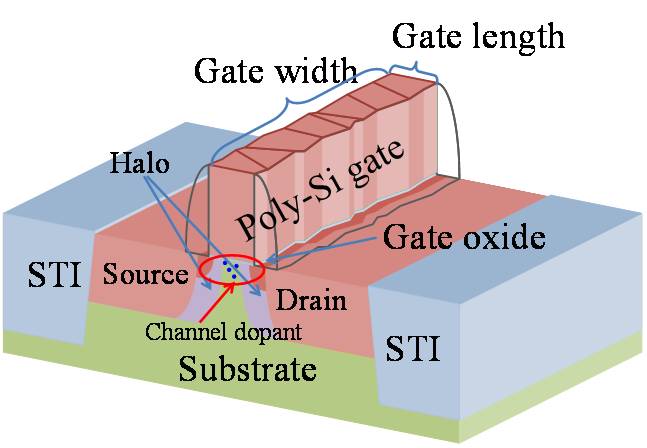
The characteristic variability of metal-oxide-semiconductor field-effect
transistors (MOSFETs) is becoming a bottleneck in achieving device scaling.
The major factor of characteristic variability is believed to be random
dopant fluctuation (RDF) in the channel. In this work to understand the
dopant behavior in MOSFET structure directly, laser-assisted atom probe
tomography (laser-APT) is applied to gate patterned MOSFET structure samples.
We found boron density in a channel underneath the gate was locally higher
than in neighboring channel region in n-type MOSFET.
Introduction
- Understanding of the three dimensional dopant distribution in MOSFET
structure is strongly required to specify the origin of characteristic variability of MOSFET.
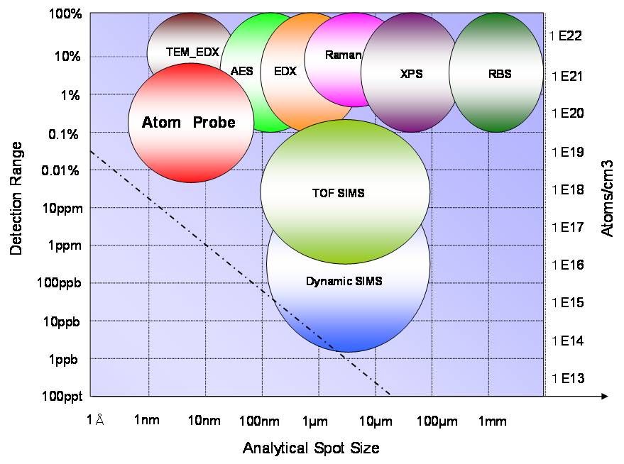
- As the sample has three dimensional structures, It is difficult to analyze the dopant distributions by SIMS. TEM-EDX is not suitable since the channel dopant concentration is lower than detection limit.
Laser-assisted atom probe tomography (APT) is possible to identify dopant positions in 3D with nearly atomic scale resolution .
- To obtain the three dimensional elemental maps of MOSFET which has gate patterned sample, and analyze the dopant distribution in gate and channel regions.
- To investigate the effect of fabricating the gate pattern and source/drain extension on channel dopant distribution.
Experiment
Sample preparation
Following three-type samples of n- and p- type MOSFETs are prepared in order to study the dopant distribution in gate patterned MOSFET structures.
Table.1 A list of prepared samples
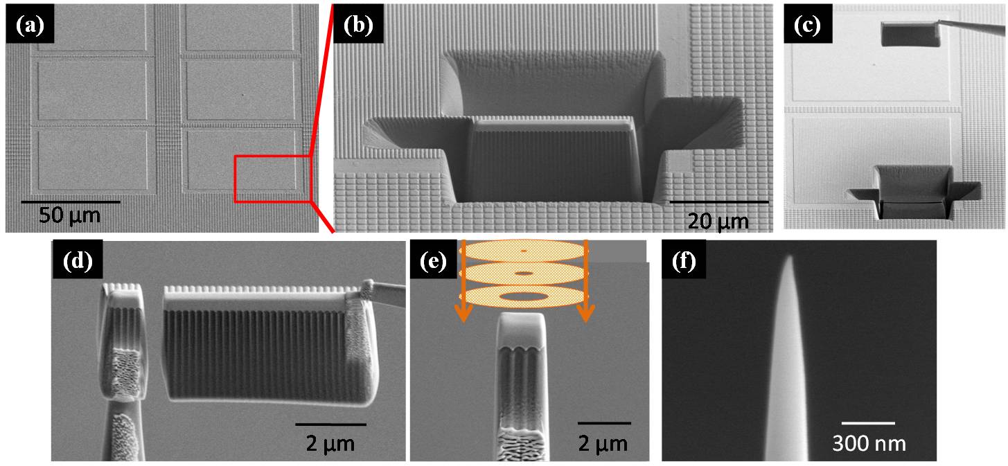
Needle specimens for APT are fabricated by FIB/SEM dual beam systems.
Following three-type samples of n- and p- type MOSFETs are prepared in order to study the dopant distribution in gate patterned MOSFET structures.
- Gate patterned MOS structures with channel, source/drain extension and Halo implantation
- Gate patterned MOS structures with channel and source/drain extension implantation without halo (to study the effect of source/drain extension implantation on the channel dopant distribution)
- Only gate patterned structures with channel implantation
Table.1 A list of prepared samples
Needle specimens for APT are fabricated by FIB/SEM dual beam systems.
- Selection of the analysis region.
- Scraping out around the site.
- Lift out using manipulator.
- Mounting the sample on micro flattop tip.
- Sharpening the specimen using annular milling patterns.
- Needle specimen for APT measurement.
Result of APT
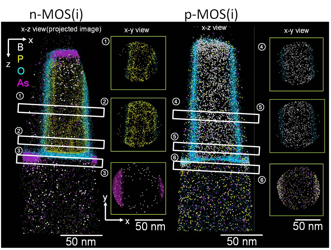
[Remarks]
- Region ① and ②
Segregation of P atoms on grain boundaries was observed. - Region ③
We observed extension of source/drain and halo structures clearly, and a high concentration of B atoms was observed at the edge of source/drain extension. - Region ④ and ⑤
Distribution of B atoms seems to uniform in the gate. - Region ⑥
We observed extension of source/drain and slightly observed P atoms implanted as halo.
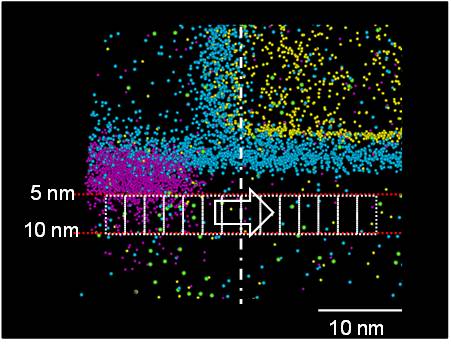
n-MOS(ii),(iii), p-MOS(ii),(iii)
We carried out APT measurements like the following (right figure) these samples. We analyzed channel dopant distributions near the edge of source/drain extensions.
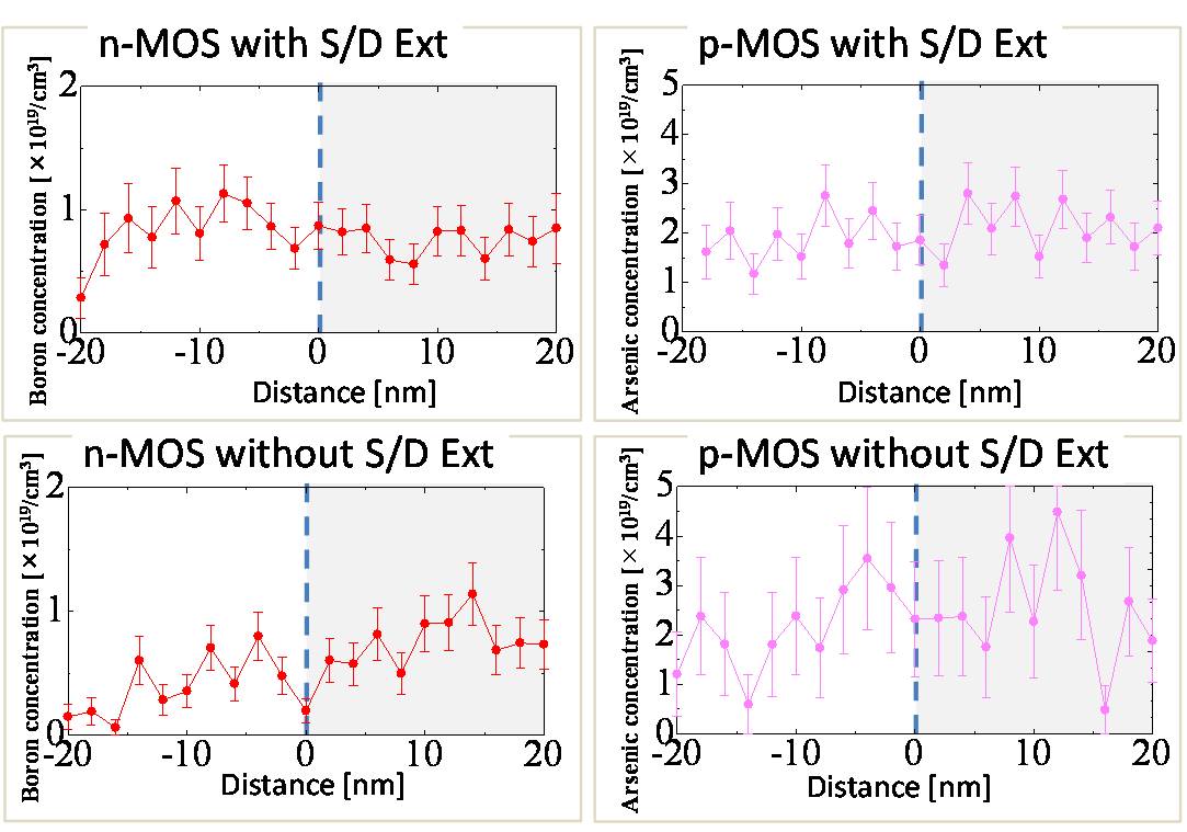
- [n-MOSFET]
-B density in the channel region underneath the gate was locally higher than that in neighboring channel region. This tendency is more remarkable in the samples without source/drain extension. - [p-MOSFET]
-There was no significant difference between the samples with and withoutsource/drain extension.